pcb-rnd knowledge pool
Thermal tool howto, for adding thermals to padstacks in pcb-rnd
| thermal_howto by Erich S. Heinzle (VK5HSE) on 2018-02-05 | Tags: howto, thermal, pin, via, padstack, clearance, menufile, menuv1 |
Abstract: Introduction to the use of the thermal tool and available thermal styles for pins, pads, vias and padstacks.
For very simple boards with no polygons (e.g. copper pours for ground planes or power planes), thermals are unlikely to be necessary.
For boards with only one polygon for either a ground plane or a power plane layer, thermals can still be avoided if clearances to surrounding copper for pins, vias and padstacks are adjusted with the usual techniques (i.e. using the {e g c} and {e g SHIFT-c} keys to adjust clearance with the pointer over the feature).
Once a design contains polygons on more than one layer for different electrical nets, simply adjusting pin clearance is no longer sufficient, since reducing the clearance to zero will short any copper polygon through which the pin, via or padstack passes.
As an aside, in designs with heat sensitive components or large copper areas, thermals may be desirable around padstacks to make manual soldering easier. A thermal reduces the amount of copper that needs to be brought up to temperature to achieve solder flow.
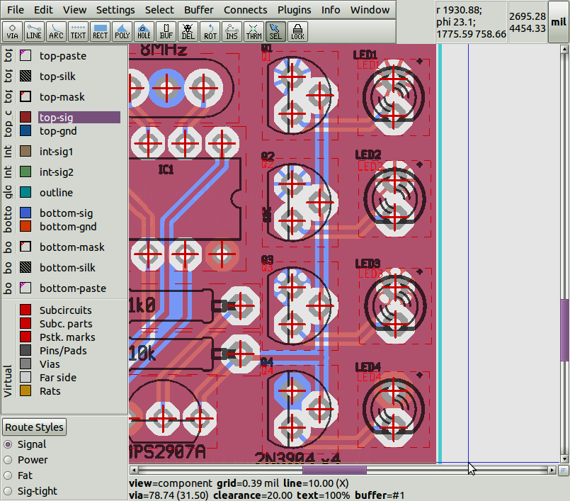
The thermal tool is present on the toolbar in pcb-rnd:
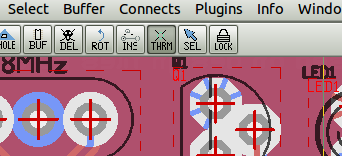
Importantly, when the thermal tool is selected, it only applies thermals to the currently active copper layer. This can be a source of confusion to new users who do not see a thermal appear when the tool is first used.
The thermal tool allows four different kinds of thermal connection to polygons.
Conceptually, the simplest type of thermal is equivalent to a zero clearance setting, with copper continuous right up to the padstack.
The next simplest thermal is a discontinuous ring of openings in the polygon.
The other two thermal types employ radial spokes to connect the feature to the surrounding polygon across a gap. These spokes can arise either from the vertices or the edges of the padstack feature.
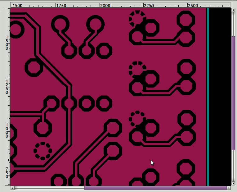
The following screenshot shows version 3 of the TV-B-Gone PCB layout which has a top copper VCC polygon and a bottom copper ground plane polygon. Thermals have been used to connect some of the pins to the ground polygon (shown in blue), and other pins to the VCC polygon (shown in red).
The different thermal styles are more readily appreciated in a screenshot from gerbv, showing the bottom copper layer
The other source of confusion for new users is how to cycle through thermal styles for a particular object.
The thermal tool is hovered over the feature, and on clicking, the existence of the thermal will be toggled the currently active layer is a copper layer. The thermal itself will be visible only when there is a polygon around the object. Removing the polygon will not remove the object's thermal bit tho: later on if a polygon is drawn again, if the thermal bit is 1, the thermal is drawn.
Further clicking while simultaneously holding the shift key will cycle through the available thermal styles.