pcb-rnd knowledge pool
Thermal on any pad
| thermals by Tibor 'Igor2' Palinkas on 2017-11-04 | Tags: announcement, padstack, via, pin, hole, pad, thermal |
Abstract: Thermals work on any pad created as a padstack.
A padstack normally includes shapes, one per layer type. "Normally", because it's optional: for example the simplest mounting hole can be a padstack that has an unplated hole and no shape at all. The hole is optional too: an smd pad typically contains shapes (e.g. for top copper, top mask and top paste but no hole.
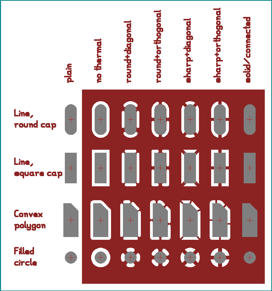
A shape is a filled circle, a line (round or square cap) or an arbitrary shaped convex polygon. The shape doesn't have to be centered at the hole.
Restrictions: only one shape per layer type, only one hole per padstack. (This is enough for vast majority of the use cases, for the rest, heavy terminals in subcircuits shall be used; a heavy terminal can contain anything that can be drawn on a PCB, without restriction.)
Since an arbitrary shaped pin or via needs to be able to make a thermal, the thermal code got upgraded to handle all the above shapes. A matrix of how they each look:
And yes, this does mean smd pads can have thermals , as long as they are done with the new padstacks, and not the old pad objects:
The ability to have different shape per layer type makes it easier to use the inner layers of dense boards: outer layers can have larger pads for better soldering of through-hole pins, while inner pads can be as small as the fab permits, to allow more traces to pass between them.
A padstack instance can be rotated and mirrored, still referring to the same central padstack prototype for the shapes. A padstack instance can have a different clearance, still using the same prototype. If a padstack instance needs to deviate, it's very cheap to copy the prototype and starts its own group with the deviations included.
There are two features I have not decided about yet, but will do in a few days:
- The "thermal style" that removes the copper shape on a specific layer group is called NOSHAPE . This again could be used for saving space on inner layers. It is accessible while cycling through thermal shapes using SHIFT-click with the thermal tool.
- Padtsack prototypes have an option for a per-shape clearance. This can be controlled on a per padstack instance basis: if the global clearance is zero, the local (per shape) clearance is used. Rationale: some IPC suggests the clearance on inner layers can be tighter than on outer layers, for various reasons. This may matter on dense boards.